I would recommend using KiCAD for PCB design. You can either export the gerber files and send them to a PCB fab or you can etch or mill the board at home.
post
Learning KiCAD is worthwhile, it's sorta becoming the Blender of PCB design. Fully open source, gaining more and more traction and getting more and more development.
For fabrication check out https://oshpark.com/ who make PCBs at hobbyist volumes. Like 3 per order. Lead free.
PCBWay / JLCPCB also looks like a decent service for fabrication, but last time I looked all their cheapest offers were not lead free. And their lead free option cost around the same as oshpark.
Good luck and Happy soldering :)
Eagle is dead. KiCAD is certainly the choice, both from starting hobbyists and for high level professionals. Order you PCBs somewhere, order stencil. Buy components yourself, solder yourself, make stencil holder from cardboard. Do not mess with assembly orders unless you've learned how it works at home. Get a fan and soldering iron, relly good tweezers (I recommend Tweezerman not made in China, absolutely best gear even though it's made for other purpose, works for electronics and electron microscopy sample handling).
Really weird fact: AI is useful for converting datasheets into kicad models, sometimes even 3D. Finally some dumb menial task worth of AI - format conversion. That's that those damn things should be used for.
If I recall, Altium has a free tier, it's my driver for work, so I use that. As for acquiring a designed board, jlcpcb is a good, inexpensive PCB fab (there are others, but jlc has been surprisingly good for my use)
If you need assembly, too, some do it, it's not cheap though.
Altium is nonfree shittyalternative for kicad by now. Don't. Especially for hobby.
For hobby work altium is quite ridiculous.
I design with Altium professionally every day. It is buggy spaghetti code that they got that way by shoving more and more productivity-centered features in there with little thought.
The libraries are a complete and utter shitshow also, which is why pretty much every company just makes their own.
It works (usually) and you can design fast with it, but for someone lightly using it for hobbies, it is a massive overkill and steep learning curve to not get any benefit over KiCAD in the end unless they want to start doing multichannel complex flex-rigid designs with mechanical linked integration.
Plus for someone wanting to just do a half hour or hour of designing in their free time, the 3-5 minute startup time would also get annoying.
Okay, I will also spend time here, please let me know any advice for newbies. Thank you for your consideration.
Have a look at EasyEDA. Browser UI, schematic and PCB design, linked to JLCPCB for ridiculously easy board creation, and if you take care to use components they have in stock out of their design libraries you can also do fully populated boards ready to go.
Here's a post I made about a solar hot water system controller using easyEDA with a few images of the board and schematic at the bottom.
I've found Fritzing pretty easy to learn and design as a hobbyist (I install with apt on my linux machine). Then PCBWay to make a small batch for pretty cheap.
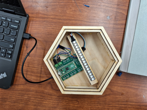
A simple board with a raspberry pi and some terminal blocks

The toner transfer method would be I think the most DIY method you can use. Make your pcbs entirely by yourself at home.
Naturally wont give you as professional a result: no silkscreen, limited to 2-layer pcbs (2 sides of a copper plate).
But it is a lot faster that having it manufactured (takes me like 1 hour for a pcb) and maybe this is debatable but it makes me feel like I have more room to make mistakes.
I am open to try this because it appeals to my sensibility. Do you have any advice to get started because I am interested and will try this if it is feasible in my garage environment? I am serious. What are the minimum materials needed/must-have requirements? I am down for this shit.
I have a laser jet printer, what kind of ventilation are we talking for the chemical? I have fume extractor on my soldering station,
Definitely look up a how to. It's been 15 years since I did this, but you'll need some photo paper to print the toner on, then use a towel and iron to transfer it to the copper clad cob. Then soak it in some FeCl for 15ish minutes. I just did this outside since it was so quick. Then like a small dremel with pcb sized bits works great for throughholes.
Awesome, yes can just do the chemical outside if volume is small and time is fast. I see there a number of how to, thank you for the inspiration, I will be trying this for sure.
This is a fine approach too. Just be aware that most modern mcu would be a hell to mount on DIY. Also, this works on literally any paper with super bold print setting.
I would recommend trying copper-based etch, it's easier to work with than FeCl3 (it's transparent, to begin with, and not as corrosive to other stuff). Edit: remember to wear goggles, all these things really destroy eyes on splash. Wash eyes for at least 15 minutes with running water if got it there.
Also, I've heard some dudes made really nice stencils for paste with some cheap hobby blade CNC tools on cardboard, there are models that have orders of mad higher precision than advertized. Never tried this myself though, lazer cut stainless steel plates from factory are just soooo good (and also a source of high quality steel in a workshop when you don't need them anymore, they make perfect wood scrapers and such)
Other than what others have suggested:
- Do get an etch resist pen. The toner occasionally, even when it goes well, might not transfer on some spots of the copper plate. So you'll need the etch resist marker to color in breaks in paths etc. and fix these little issues.
- The acid or whatever you use to etch away the copper might not work on some spots. Leading to shorts or otherwise unwanted connections. So do check with a multimeter the paths and pads that are close to make sure there arent shorts. You can scratch away unwanted copper with a blade.
I dont think theres much more to add, its quite a simple process. Have fun :)
On single sided PCBs, you can do a toner transfer on the component side for a silkscreen. You can apply solder mask too, but it's a rather messy process.
oh, and do not be afraid of surface mount. It's actually easier than it looks, especially if you were smart and did order a stencil (otherwise it's a toothpick and paste, nothing too hard, just... so slow that paste will dry out).
paste recommendation: ChipQuick. Surprisingly, stuff from hobby shop works better than many professional products, even in professional settings. I had my team leaving spatula on stencil printer for months, just warm it up a but and it's like new. Magic.
Kicad and YouTube videos on it. Its pretty popular for home and semi-professional
all 27 comments